

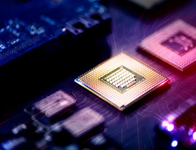
Intel has outlined new advances in its semiconductor manufacturing roadmap, announcing that its Intel 18A-P process technology has entered risk production while also unveiling research aimed at extending chip scaling beyond current-generation transistor designs.
At the 2026 VLSI Symposium, Intel Foundry provided an update on its advanced manufacturing technologies, highlighting progress on its Intel 18A-P process node and revealing several long-term research projects designed to support future semiconductor development.
The company said Intel 18A-P, an enhanced version of its Intel 18A manufacturing process, has entered risk production, meeting a schedule previously shared with customers and industry partners. According to Intel, the new node delivers up to 9% higher performance at the same power level or reduces power consumption by as much as 18% while maintaining equivalent performance.
Engineers at the symposium detailed several technology improvements incorporated into the process. These include a new “Power Boost” transistor design intended to increase drive current and operating frequency, thermal resistance improvements ranging from 20% to 40%, and lower via resistance to improve electrical efficiency within chips. Intel also noted that Intel 18A-P remains compatible with existing Intel 18A design rules, allowing customers to reuse established design flows and intellectual property.
Beyond the manufacturing update, Intel researchers presented findings related to gate-all-around transistor technology and backside power delivery, two technologies introduced with Intel 18A. The company reported that these approaches can reduce routed chip area, lower voltage fluctuations, and improve power efficiency and performance in future processor designs.
Intel also used the event to highlight several research initiatives focused on extending semiconductor scaling. Among them were demonstrations of complementary field-effect transistor (CFET) inverters featuring vertically stacked transistor structures, integration of gallium nitride power devices with silicon logic on 300mm wafers, and a subtractive ruthenium interconnect approach aimed at reducing capacitance and improving chip performance as device dimensions continue to shrink.
The announcements provide a snapshot of Intel Foundry’s current manufacturing progress and its efforts to develop technologies that could support future generations of advanced semiconductor products.
Source: Intel Foundry Details Process Milestones and Future Innovation at VLSI Symposium – Intel Newsroom