IBM has introduced what it describes as the world’s first sub-1 nanometer semiconductor technology, marking a significant research milestone that could shape the next generation of artificial intelligence, cloud computing and high-performance processors.
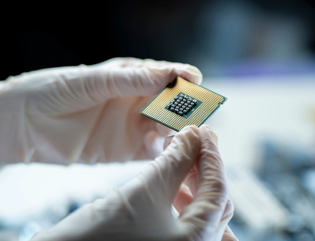
IBM has announced a breakthrough in semiconductor research with the debut of a 0.7-nanometer (7-angstrom) chip technology, pushing chip design beyond the one-nanometer threshold for the first time. The development comes as the semiconductor industry searches for new ways to improve computing performance while overcoming the physical limitations of conventional transistor scaling.
At the center of the innovation is Nanostack, a newly developed three-dimensional transistor architecture. Unlike existing designs that primarily scale transistors horizontally, the new approach vertically stacks and staggers transistor layers, allowing significantly higher transistor density within the same chip area. IBM said the architecture also enables different material combinations across stacked layers, helping optimize both performance and power efficiency.
The research chip packs nearly 100 billion transistors onto a chip roughly the size of a fingernail, almost doubling the transistor density achieved by IBM’s 2-nanometer technology introduced in 2021. According to the company, the design is projected to deliver up to 50% higher performance or 70% greater energy efficiency compared with its previous 2 nm node technology, making it particularly relevant for compute-intensive workloads such as generative AI, cloud infrastructure and advanced electronic systems.
IBM also reported progress in memory scaling, stating that the Nanostack architecture enables 40% SRAM scaling, an advancement that could support future AI processors requiring larger and faster on-chip memory.
The technology remains in the research stage and is not yet intended for commercial production. IBM, however, believes the new architecture provides a roadmap for continued semiconductor scaling over the next decade and estimates that the earliest commercial adoption of Nanostack-based technology could begin within five years.
The announcement reinforces IBM’s long-standing role in semiconductor research as the industry seeks new architectural approaches to sustain advances in computing performance beyond traditional process scaling.
Source: This article is based on an official press release issued by IBM
IBM Debuts World’s First Sub-1 Nanometer Chip Technology